PCB results viewer
Two real open-hardware boards, read from their KiCad files. Pick a copper layer to see its solved voltage drop, current density and temperature, or switch to 3D and explode the stackup; click a red cut marker for the trace cross-section, or open the via cell.
Layers: drag to pan, wheel or pinch to zoom. 3D: drag to orbit, shift- or right-drag to pan. Every view states its source under the plot. What these results show
More demos
All demos →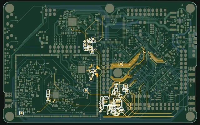
What each parts-list change did to the board
Every parts-list change in real open-hardware projects, traced to what it did to the circuit board.
162 commits read Simulation coupling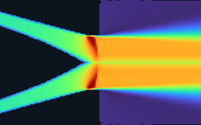
A jet engine, solved: compressible CFD, chemistry and a full start-up
Compressible CFD, combustion chemistry and a full start-up in one loop, every number traced to its run.
1,098.5 K vs 1,100 K target Transaxle checks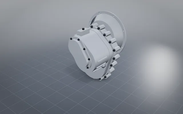
The checks your checker forgets, run on a car transaxle
Tolerance stacks and a full fastener audit catch a bearing preload problem as drawn, then prove the fix.
175 parts · 30 fasteners Drawings to STEP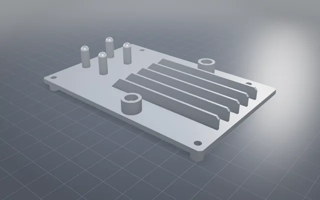
Manufacturing drawings in, STEP out, checked against the original
Real manufacturing drawings become exact 3D models, each matched against the official model.
6 of 6 NIST parts matchedBuild your own part with NativeCAD
Free for education and makers with a registered key · $200 per seat per year · Kernel SDK for products.