Pass
UL 796 construction
meets the fab's UL-recognized construction
One run over your board returns a single readiness report: UL 796 construction, IPC-6012 class, coupon predictions, spacing and ampacity, each with a green, amber or red line and the one change that fixes it. Here it is on the ULX3S FPGA board.
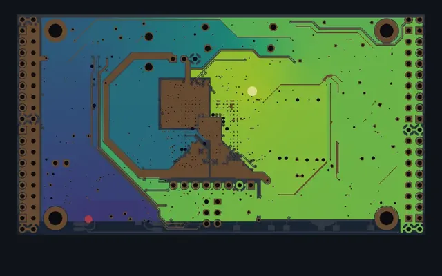
Every via on the ULX3S, coloured by whether it keeps its Class 3 ring: amber ones need a wider pad. The chips switch each check on and off; tap a via or a marker for its numbers and its report line. Drag to pan, pinch or wheel to zoom.
meets the fab's UL-recognized construction
Class 2: 100% via ring retention under the fab drill tolerance
Class 3: 77.9% ring retention as drawn, 100% with the pad change
9 via structures predicted to pass solder float, 6x reflow and IST; fewest IST cycles 1424 against 1000 required
+5V to GND: clearance 0.2 mm, 0.1 mm required
vccio33 0.48 A: pass; core1v1 0.3 A: pass
Steinberg: all 7 assessed parts within their allowable deflection, lowest margin 5.62x (U1); JESD22-B111 drop: U1 1927 microstrain over the 1500 microstrain limit
Not assessed: no cycles-to-failure is given for any part. This report has no solder-joint life model and no sourced package or laminate CTE to run one on, and it does not invent them
100% Class 3 with one change
Widen the pads on 510 of the 554 vias (table below). Flip the board between how it is drawn and with the change: the 510 amber rings go green. Tap any via for its numbers.
With the change, all 554 vias keep their ring: 100% Class 3 retention. Tap any via.
400 simulated drill hits on one of the 488 Ø0.2/0.419 vias, with the fab's ±0.075 mm drill and ±0.05/0.075 mm layer registration. A hit that reaches into the shaded band has lost its 0.05 mm Class 3 ring: 102 as drawn, 0 with the wider pad.
Smallest annular ring over the simulated drill hits, weighted to all 554 vias. As drawn, part of the amber distribution sits left of the Class 3 line; with the change all of the green sits to its right.
| Vias | Drill | Pad today | Pad for Class 3 | Keep ring now | After |
|---|---|---|---|---|---|
| 488 | 0.2 mm | 0.419 mm | 0.55 mm | 75.2% | 100% |
| 13 | 0.3 mm | 0.6 mm | 0.65 mm | 99.5% | 100% |
| 5 | 0.25 mm | 0.5 mm | 0.6 mm | 91.3% | 100% |
| 3 | 0.254 mm | 0.5 mm | 0.604 mm | 91.3% | 100% |
| 1 | 0.254 mm | 0.454 mm | 0.604 mm | 60% | 100% |
Predicted interconnect stress test (IST) life for each via structure on the board, against the 1000 cycles Class 3 qualification asks for. All 9 also pass solder float and six reflows.
The weakest structure is the Ø0.2 mm via with a 0.419 mm pad, 488 of them on the board: 1424 cycles against 1000. Open it to see the plated barrel in cross-section at the 260 °C reflow peak, coloured by stress, with the barrel knee where the pad meets the hole one tap away.
ULX3S by Radiona / EMARD, modified MIT. Design checks against the standards, not certificates issued by their bodies.
IR drop, impedance, weave skew, eye diagrams and via life, read straight from your board file.
Eyes open at 56 Gbps BOMblame pilot
Every parts-list change in real open-hardware projects, traced to what it did to the circuit board.
162 commits read Simulation coupling
Compressible CFD, combustion chemistry and a full start-up in one loop, every number traced to its run.
1,098.5 K vs 1,100 K target Drawings to STEP
Real manufacturing drawings become exact 3D models, each matched against the official model.
6 of 6 NIST parts matchedFree for education and makers with a registered key · $200 per seat per year · Kernel SDK for products.